|
|
Digitial A21164
Hardware Overview
CPU Architecture of the DEC PWS
500au:The Alpha 21164 has the following
features:
- 64 bit RISC architecture
- fully pipelined
- superscalar 4-way instruction issue (2 integer
pipelines, 2 floiting-point pipelines)
- 32 integer registers (+ 8 PALshadow
registers)
- 32 entry, 64 bit floating-point register
file
- 8 KB, direct-mapped, L1 instruction cache
(onchip)
- 8 KB, direct-mapped, write through L1 data
cache (onchip)
- 96 KB, 3-way, set-associative, write-bake L2
data and instruction cache (onchip)
- supports optional board-level L3 cache (1 MB -
64 MB)
Scheduling and Issuing
Rules:
- There are 2 integer pipilines (E0 and E1), a
floating-point add (FA) and a floating point
multiply pipeline (FM).
- Load are executed in E0 or E1. Stores in E0.
Loads and Stores cannot be issued simultaneously.
IBranches are issued in E1, IAdds in E0 or E1,
IMults and shifts in E0. Fadds are issued in FA,
Fdiss in FA, Fmul in FM, FBranches in FA.
- It is possible to issue simultaneously 4
instructions in a INT16 (natually aligned block of
16 Bytes) to the 4 pipelines as far as the
resources for the instructions are available.
- Out-of-Order Issues are not performed. Therfore
if the issue of one of the instructions in the
INT16 block is not possible the following
instructions in the block are also delayed, even if
their resources are available.
- The next INT16 block is issued when all
instructions of the previous INT16 block are
issued.
Sources of Latency (Processor
Stalls):
- Cache misses
- TLB misses
- Register dependencies
- Branch mispredictions
- Memory barrier instructions
- Replay traps
- Cache coherence protocol (mainly in
multiprocessor systems)
Memory Architecture of the DEC PWS
500au (Alpha 21164):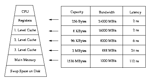 Memory Architecture of the DEC PWS 500au
Instruction Translation Buffer
(ITB):
Memory Architecture of the DEC PWS 500au
Instruction Translation Buffer
(ITB):
- Fully associative TLB.
- 48 entries, not-last-used replacement.
- Each entry can map 1, 8, 64, or 512 contiguous
pages of 8 kB size.
Data Translation Buffer
(DTB):
- Fully associative TLB: 43-bit VA --> 40-bit
PA.
- 64 entries, not-last-used replacement.
- Each entry can map 1, 8, 64, or 512 contiguous
pages of 8 kB size (i.e., 8 kB, 64 kB, 512 kB, 4
MB). The size of the each mapping is specified by
hint bits stored in the entry.
- 1 cycle for address translation: pipeline stage
S4.
- Address translation is done in parallel with
data cache access.
- Dual-ported, i.e., 2 address translations per
cycle are possible.
- ITB and DTB implement 7-bit address space
numbers (ASNs) per entry to indicate the context
for which the address translation entry is
valid.
- ITB and DTB misses have significant penalties,
i.e., PALcode entry and, potentially, memory
accesses.
- TLB miss latency: > 20 cycles! (Assumption
of a study on a 300 MHz Aplha [5])
L1 Instruction Cache:
- On chip, direct mapped, 8 kB, 32-byte
blocks.
- Part of instruction unit.
L1 Data Cache:
- On chip, direct mapped, 8 kB, 32-byte blocks,
write through.
- Dual-read-ported, i.e., 2 reads per cycle are
possible; single-write-ported.
- Non-blocking, i.e., does not block to serve a
miss.
- Latency: 2 cycles! Load: cache read is done in
S4 and S5, data is loaded into register in S6.
Store: cache hit is determined in S4 and S5, data
is stored into cache in S6.
- This latency figure assumes that the
instruction after a load is an operate instruction;
the data fetched from the L1 cache is directly fed
into the I or FP pipeline. The data is available in
a register 3 cycles after the load.
- Example of instruction stream and optimal
execution time (L1 cache hit):
Cycle i: LDL R2, 0 (R1)
Cycle i+1: NOP
Cycle i+2: ADDL R2, R3, R4
Memory Load and Store Merge
Logic:
- Connects (or, decouples) L1 caches and L2
cache.
- 2 components: MAF and WB.
- Miss Address File (MAF):
- Buffers loads that missed in the L1
caches.
- Merges multiple loads into same 32-byte block
(under certain restrictions), up to 2 loads per
cycle.
- Capacity:
6 entries (32-bytes each) for 21 different data
loads;
4 entries for instruction fetches.
- Write Buffer (WB):
- Buffers stores that missed in the L1 data
cache.
- Merges multiple stores into same 32-byte
block, 1 store per cycle.
- Capacity: 6 entries (32-bytes).
- Stops merging when block write sent to L2
cache.
- Holds entry until completion is signaled by
L2 cache.
- Connection to L2 cache:
- MAF and WB send one (merged) load or store
as a 32-byte block access to L2 cache every 2
cycles.
- Priorities: data load, store, instruction
fetch.
- Effects of these components:
- Some L1 cache misses may see only part of
effective L2 cache access latency.
- L2 cache bandwidth is saved through
buffering and merging.
- Data accesses may be finished out of order,
however, access ordering as given by the
instruction stream is guaranteed.
Memory Barrier Instructions and Replay
Traps:
- Memory Barriers cause all outstanding memory
accesses to be finished.
- Replay Traps are generated if an access would
cause a buffer to overflow and cause the access to
be repeated later on.
- Effect: noticeable memory access latency
penalty!
L2 Cache:
- On chip, 3-way set associative, 96 kB, write
back, unified I&D, single-ported.
- Configurable to handle 64-byte blocks or
32-byte subblocks.
- Writes back to off-chip cache only the modified
16-byte data words.
- 128-bit read and write paths to execution units
and L1 caches; 32 bytes are transferred in 2
successive cycles.
- Load access: data are directly transferred to
the I or FP pipeline, then to L1 data cache, then
written into register (called "fill").
- A "fill" of the I pipeline, L1 cache and
registers from L2 cache causes 2 or 3 empty cycles
to be allocated so that the L1 cache port is
available!
- Minimum load latency: 8 cycles! (I.e., the next
instruction depending on the register value can be
issued 8 cycles later.)
- Minimum store latency: 5 cycles!(?) (Due to
store buffering, the CPU does not encounter this
latency, though.)
- Latencies are higher if there are arbitration
conflicts for the L2 cache.
Bus Interface Unit File
(BAF):
- Between L2 and L3 cache.
- Buffers memory accesses that missed in L2
cache.
- Merges read requests to 32-byte blocks within
the same 64-byte block.
- 2 entries.
- Effect: may lower average L3 cache access
latency.
L3 Cache:
- Off chip, control is on chip.
- Direct mapped, write back.
- 1
- 64 MB, typical 2 MB; optional in some
machines.
- Block size configurable to 32 or 64 bytes.
- Minimum load latency: 12 cycles!(?)
Main Memory:
- Example: Personal Workstation with 21174 Memory
Controller.
- SDRAM memory, 66 MHz system clock.
- 4 cycles of the 128-bit data bus for a 64-byte
L2 cache line fill.
- Minimum load latency: 75 cycles @ 500 MHz (10
bus cycles = 150 ns)!(?)
Latency Summary:
| Type of access |
[1]-[4] |
[5] |
| TLB miss |
? |
> 20 cycles |
| L1 cache |
2 cycles |
2 cycles |
| L2 cache |
> 8 cycles |
7 cycles |
| L3 cache |
> 12 cycles |
21 cycles @ 300 MHz |
| Main memory |
> 75 cycles |
80 cycles @ 300 MHz |
| C-to-C transfer |
? |
125 cycles @ 300 MHz |
Miscellaneous:
- The Alpha instruction set has several cache
related instructions [6]:
- FETCH - Prefetch Data:
- Hint to implementation. Implementation may
optinally attempt to move all or part of a 512
byte block of data to a faster-access part of
the memory hierarchy. These instructions are
"architecturally optional" [1]. In the 21164,
"partial hardware implementation is provided"
[1].
- FETCH_M - Prefetch Data, Modify
Intent:
- Same as FETCH, but gives the additional
hint that modifications to the data block are
anticipated.
- ECB - Evict Data Cache Block:
- Makes a particular cache location available
for reuse by evicting and invalidating its
contents.
- WH64 - Write Hint 64 Bytes:
- Provides performance hint that the contents
of the 64-byte block will never be read again,
but will be overwritten in the near
future.
- Causes for stall cycles in commercial workloads
[5]:
- Stall cycles are about evenly divided
between instruction
- and data-related.
- About half of memory system stalls are hits
in L2 and L3 caches.
- L2 cache hits mostly account for > 20%
of overall execution time.
- Branch mispredictions and reply traps
account for about 10%-20% of ex. time.
Related Information on the Web:
References:
- [1]
- Digital Equipment Corporation. Digital
Semiconductor 21164 Alpha Microprocessor Hardware
Reference Manual. EC-QP99B-TE. Feb. 1997.
- [2]
- J.E. Edmondson et al. "Internal Organization of
the Alpha 21164, a 300-MHz 64-bit Quad-issue CMOS
RISC Microprocessor". Digital Technical Journal,
vol. 7, no. 1, 1995, pp. 119-132.
- [3]
- K.M. Weiss, K.A. House. "DIGITAL Personal
Workstations: The Design of High-performance,
Low-cost Alpha Systems". Digital Technical Journal,
vol. 9, no. 2, 1997, pp. 45-56.
- [4]
- R.C. Schumann. "Design of the 21174 Memory
Controller for DIGITAL Personal Workstations".
Digital Technical Journal, vol. 9, no. 2, 1997, pp.
57-70.
- [5]
- L.A. Barroso, K. Gharachorloo, E. Bugnion.
"Memory System Characterization of Commercial
Workloads". To appear in: Proc. 25th Int'l. Symp.
on Computer Architecture (ISCA-25), June 1998.
- [6]
- Digital Equipment Corporation. Alpha
Architecture Handbook. EC-QD2KB-TE. Oct. 1996
|
|